A Covert Startup Believes It Has Solved the Memory Crisis
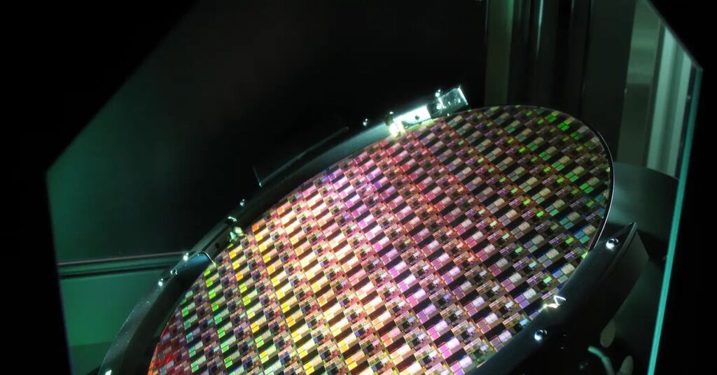
Kepler has announced enhancements in SRAM density by utilizing ferroelectrics, enabling data to be read and written at lower voltages compared to conventional methods used for data processing and storage in semiconductors. This advancement was achieved through the development of a novel low-voltage composite material that complements the ferroelectric technology.
According to Sasi Manipatruni, a cofounder and chief technology officer of Kepler, the team experimented with 35 different iterations of composites before identifying a material class that would simplify and reduce the costs of manufacturing memory chips.
“Once we discovered a solution to the physics issue—specifically, the physical constraints for HBM—we developed an innovative material that increases the memory capacity between chips,” he states.
During early collaborations with GlobalFoundries, Kepler claims it converted a fabrication facility into a “next-generation” setup in just eight months, significantly shorter than the average 24-month timeline.
“Our goal is to maximize the capabilities of existing fabs and architectures, pushing them to their physical limits,” Olaosebikan explains.
Essentially, Kepler believes that any extra expenses incurred from new materials or reconfiguring current fabs will be minimal compared to the $20 billion to $40 billion required to construct new facilities equipped with state-of-the-art machinery worth hundreds of millions.
Waiting to Scale
Kepler Computing faces a lengthy journey before achieving full-scale production—if they reach that milestone. So far, the company has tested its technology on approximately 2,000 wafers. The startup plans to deliver its first samples of HBM chips later this year, increase production in Singapore next year, and commence chip manufacturing in the US by 2028.
Kaste, an executive at GlobalFoundries, expresses confidence that the “fundamental breakthroughs have been made. The next step is to achieve positive results on thousands of wafers and millions of devices.”
He highlights that a significant challenge with the material system Kepler is using is the inclusion of iron in its composite. “Iron is a challenging contaminant for a production facility. Thus, Kepler’s solution must be processed on dedicated equipment or entirely encapsulated to prevent contamination,” he adds.
“The key lies in maintaining the material isolated throughout our production flow,” Kaste remarks.


Rajat Sharma
https://in.linkedin.com/in/rajat-mediaHelping D2C Brands Scale with AI-Powered Marketing & Automation 🚀 | $15M+ in Client Revenue | Meta Ads Expert | D2C Performance Marketing Consultant