The Outrageously Geeky Intel Gamble That Could Generate Billions
It remains an exceptionally difficult endeavor. “Packaging isn’t merely about saying, ‘I want to produce 100,000 wafers each month,’” notes Jim McGregor, a seasoned chip industry analyst and founder of Tirias Research, referencing the continuous flow of chips through various production stages. “Ultimately, it hinges on whether Intel’s [packaging] fabs can secure agreements. An increase in their operational expansion would signal that they’re making progress.”
Recently, Anwar Ibrahim, the Prime Minister of Malaysia, announced on Facebook that Intel is expanding its Malaysian chip manufacturing facilities, established in the 1970s. Ibrahim mentioned that Naga Chandrasekaran, the head of Intel’s Foundry, had “detailed plans to initiate the first phase” of expansion, which will focus on advanced packaging.
“I am pleased with Intel’s decision to start operations for the complex later this year,” stated a translated version of Ibrahim’s post. An Intel spokesperson, John Hipsher, confirmed that the company is enhancing its chip assembly and testing capacity in Penang, “in response to increasing global demand for Intel Foundry packaging solutions.”
Package Store
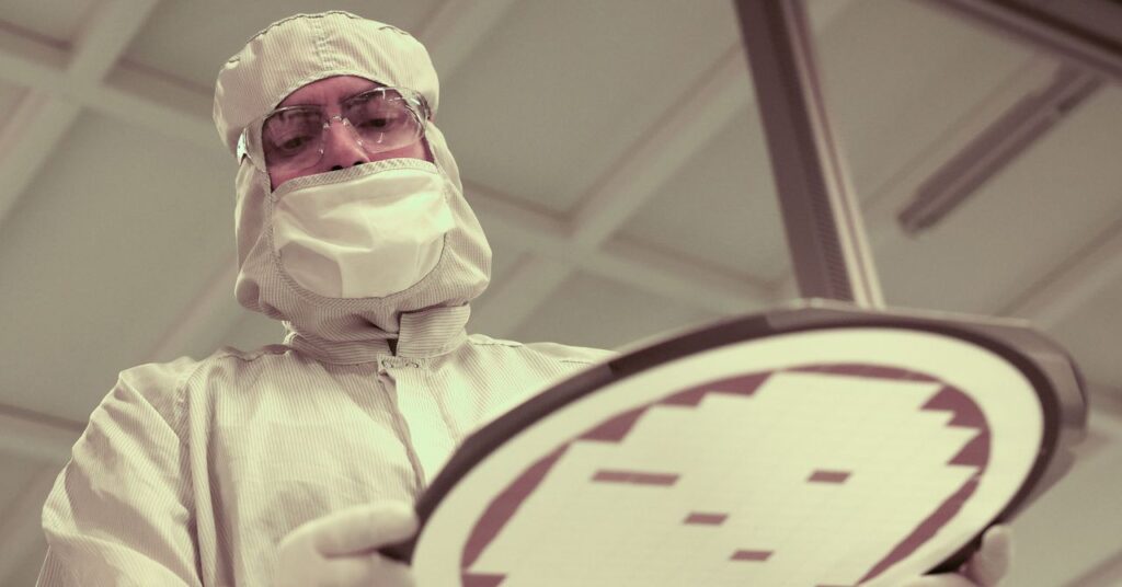
According to Chandrasekaran, who assumed leadership of Intel’s Foundry operations in 2025 and spoke exclusively with WIRED for this report, the phrase “advanced packaging” didn’t even exist a decade ago.
Chips have always needed some form of integration for transistors and capacitors that manage and store energy. For many years, the semiconductor industry concentrated on miniaturization—reducing component size on chips. As global computing demands heightened in the 2010s, chips became denser with processing units, high-bandwidth memory, and necessary connective components. Eventually, chipmakers adopted a system-in-packages or package-on-package approach, stacking multiple elements to maximize power and memory on the same surface area. This transitioned from 2D stacking to 3D stacking.
TSMC, the leading semiconductor manufacturer globally, began offering packaging technologies like CoWoS (chip on wafer on substrate) and later SoIC (system on integrated chip) to its customers. Essentially, the proposition was that TSMC would manage not just the front end of chip-making—the wafer process—but also the back end, where all the chip technology is assembled.
At that time, Intel had lost its chip manufacturing edge to TSMC but continued to focus on packaging. In 2017, it launched a process called EMIB, or embedded multi-die interconnect bridge, which was notable for minimizing the actual connections, or bridges, among the components within the chip package. In 2019, it unveiled Foveros, an advanced die-stacking method. The company’s next packaging advancement, EMIB-T, was a significant leap forward.
Introduced last May, EMIB-T aims to enhance power efficiency and signal integrity among all components on the chips. A former Intel employee familiar with the company’s packaging initiatives shared with WIRED that Intel’s EMIB and EMIB-T are intended to provide a more “surgical” approach to packaging chips compared to TSMC’s strategy. Like many chip innovations, this is expected to be more energy efficient, conserve space, and ideally, reduce costs for customers in the long run. The company anticipates EMIB-T to start production in fabs this year.

Rajat Sharma
https://in.linkedin.com/in/rajat-mediaHelping D2C Brands Scale with AI-Powered Marketing & Automation 🚀 | $15M+ in Client Revenue | Meta Ads Expert | D2C Performance Marketing Consultant